Challenge
to Nanotechnology!
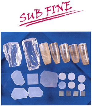 |
We
offer super thin substrates( product name:?gSUB?@FINE?h)prepared by
our unique special polishing technology. We made a breakthrough and
prepare ultra super thin substrate for the nano-technology world.
Compared to conventional substrates, ?g SUB FINE?h minimizes internal
stress, such as cracks, bend and precess deformation. |
|
|
We
h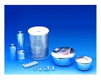 ave
started to sell super ultra high purity MBE Aluminium, manufactured
by Pechiney Mercus Plant, Groupe Arnaud Electronics. This Aluminium
is the purest in the world(6N5) with extremely low level of oxygen.
It is highly recommended to use for MBE. ave
started to sell super ultra high purity MBE Aluminium, manufactured
by Pechiney Mercus Plant, Groupe Arnaud Electronics. This Aluminium
is the purest in the world(6N5) with extremely low level of oxygen.
It is highly recommended to use for MBE. |
| Items |
�r�t�g�o�|�`�h |
Shape |
Dimensions |
Price |
| Purity |
�X�X�D�X�X�X�X�T�� |
�q���� |
�P�O���~�S�O�k���� |
Estimate |
| �U�m�T |
�r�������� |
�U���~�Q�O�k���� |
Estimate |
Please contact us with your size requirement.
We also manufacture and sell the other MBE materials, such as
�f����`���A�h���A�o�A�a���A�r���A�s���A�r���A�y��.
|
Lead
Magnesium Niobate-Lead Titanate

A New Piezocrystal for Next-Generation Electromechanical Transducers
|
 |
| �@Structure |
�@R3m |
|
�@Dielectric
loss |
�@tan
ð<0.9 |
| �@Density |
�@8.1g/cm3 |
|
�@Composition |
�@near
the morphotropic
�@ phase boundary |
�@Piezoelectric
�@Coefficient d33 |
�@>2000PC/N |
|
�@Curie
�@temperature |
�@135�`150�� |
�@Coupling
�@Constant |
K33 |
�@>92% |
|
�@Standard
size |
�@25�~25�~1mm3
�@etc |
| Kt |
�@59�`62% |
|
| K33' |
�@84�`88% |
|
��Properties
are somewhat dependant on the composition of solid solution so the
choice of composition may require a compromise in desired properties.
|
 |
|
| |
 |
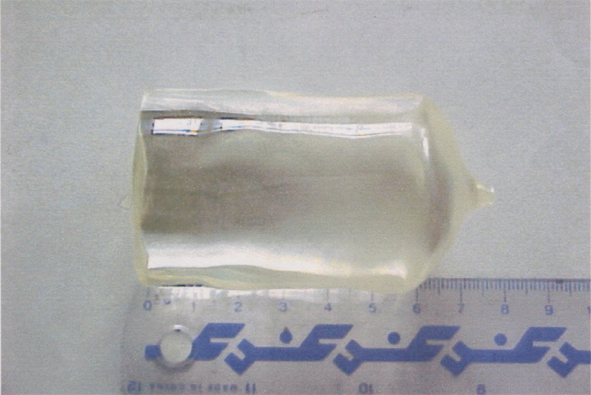
��Furuuchi Chemical
has successfully developed aqueous Titanium compounds, "TAS�FINE,"
that are completely different from the standard Titanium compound.
"TAS�FINE" is stable, neutral and water soluble.
This material is unique, easy to handle and useful in a wide
variety of applications. |
Products
Name: TAS�FINE
Chemical Formula: Titanium peroxi citric acid ammonium tetrahydrate
Composition: (NH4)4[Ti2(C6H4O7)2(O2)2]�4H2O
Molecular Weight: 680.16
Ti Contents: Ti < 20%
|
| Sample
Price |
| Ti -
5% aqueous solution |
Ti - 20%
powder |
| 100ml |
100g |
| 500ml |
500g |
| 1,000ml |
1kg |
|
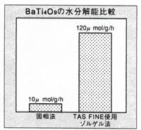
Comparative bar chart for BaTi4O9 water solubility
| Physical
Properties |
| Decomposition temperature |
350�� |
| Solubility |
Soluble in water |
| Boiling point (aqueous solution) |
100�� |
| PH (aqueous solution) |
Neutral |
| Dielectric constant (TiO2) |
117 (at room temperature) |
| Other property |
Absorb ultraviolet ray |
| Appearance |
Yellow clear liquid, Yellow powder |
  �@�@�@�@ �@�@�@�@
|
|  �@�@ �@�@
We are now
have on sale Dye Solar Sensitizer and various display materials
from Solaronix SA, a Swiss company. These unique materials
will allow you to prepare Solar cells more easily. |
|
Item |
Quantity |
Price |
Application |
| Ruthenium�@Dye |
Ruthenium
- 470
Ruthenium - 505
Ruthenium - 535
Ruthenium - 535_bisTBA
Ruthenium - 620 |
100mg,
500mg, 1g, 2g�@�c�@etc
100mg, 500mg, 1g, 2g�@�c�@etc
100mg, 500mg, 1g, 2g�@�c�@etc
500mg, 1g, 2g, 5g �@�@�@�c�@etc
100mg, 500mg, 1g�@�@ �@�c�@etc |
Estimate
�V
�V
�V
�V |
Electronic
circuits
�V
�V
�V
�V |
Nanocrystalline
Metal�@Oxide |
Ti
- Nanoxide - D
Ti - Nanoxide - T
Ti - Nanoxide - HT |
10g,
50g, 100g, 200g�@�@�c�@etc
10g, 50g, 100g, 200g�@�@�c�@etc
10g, 50g, 100g, 200g�@�@�c�@etc |
Estimate
�V
�V |
Transparent
micro crystals
�V
�V |
Redox�@
Electrolytes |
Iodolyte
- TG50
DMP - �U |
5ml,
10ml, 20ml, 50ml, 100ml�cetc
10g, 20g, 50g�@ �@�@�@�@�@�@�@�@�cetc |
Estimate
�V |
Electrolyte
Electrolyte solution |
| Sealing�@Materials |
Amosil
- 4 |
20g,
50g �@�@�@�@�@�@�@�@�@�@�@�@�cetc |
Estimate |
Sealant |
|

|
 |
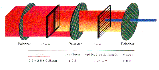
PLZT
Optical Shutter Arrays in practical use as printer heads and
photo imaging are expected to find applications in the fields
of image engineering and optical data communication.
We offer Optical Shutter and Processed substrates, those of
which minimize processing damage and optical strain and make
the best use of the capabilities of the materials.
|
 �@Prototype
Product �@Prototype
Product
Electrostatic
Bonding Device
or High Temperature Static Electricity Bonding Device
|
|
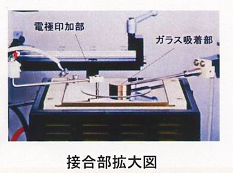
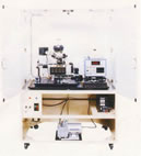
For
laminating wafers and creating various sensors and actuators!
The device allows the lamination
of Si wafers and Pyrex glass in anode bonding, which is essential
in micro-machining technology.
Place Si wafer and Pyrex glass in direct contact with one
another and heat to 400��, impress a negative charge of several
hundreds volts on the glass side, and electrostatic attraction
allows chemical bonding at the interface. |
| Specifications |
| Functions |
Bonding Wafer Size
|
�E�Q�g�i�ӂT�P�����j�`�ӂS�h�i�ӂP�O�O�����Ӂj |
| Heater |
�ETemperature setting
range�F�O�`�S�T�O���iPID control system�j |
| �ETemperature distribution�F�}�P��
�iLess than �P�P�O���� ��face on the heater�j |
| �EMaterial�@ �FBrass�@�i
Casting heater�j |
| Direct-current power
supply |
�EVoltage control ranger
�F
�O�`�P�O�O�O�� |
| lass Absorption�@ |
�EUltimate vacuum�@�F
Vacuum pumping range�@���T�O Torr |
| Outside Dimension |
�@ |
�P�O�O�Omm�iW�j�~�U�O�Omm�iD�j�~�P�T�W�Umm�iH�j |
| Weight |
�@ |
Nominal �P�T�Okg�iExcluding
floor-type vacuum pump) |
| Power Source |
�@ |
AC�P�O�OV�A�T�OHz�A�Q�OA |
|
Safety Precautions:
Do not install the device in wet, dusty and oily environments
to avoid fire, electrocution or other accidents |
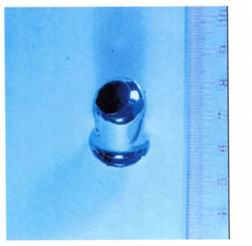
| Pb1-xSnxTe Single crystal�ix=0�`0.2�j |
| We
have started to manufacture and sell PbSnTe single crystal as
use of infrared lasers and infrared detectors. Compared to HgCdTe
single crystal, PbSnTe single crystal has less dark current
and no toxicity. It is therefore, better on environment. |
��Single
Crystals Properties and Specifications
| �@Orientation |
�@<100>
(other orientations possible) |
| �@Form |
�@20���`25��mm�@Thickness�@0.5t�`optional |
| �@Dislocation Density |
�@103�`104cm-2 |
| �@Electrical Properties |
�@P-type
or�@N-type |
| �@Carrier Concentration |
�@1017�`1019cm-3 |
|
��Applications
�@�EInfrared
Lasers
�@�EInfrared
Detecors
�@�EHgCdTe
substitute |
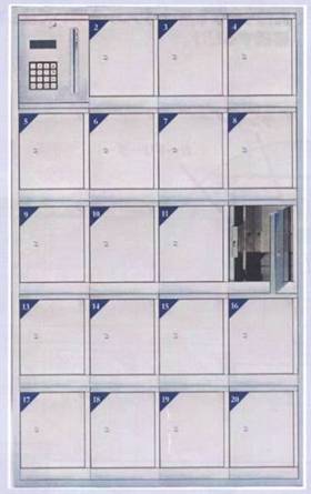 |
"New
Product"
FINE CABINET
|
��Storage
Management System for Property,
Valuables & Chemicals ��
|
| FINE CABINET provides
security, control and management for property, valuables
and chemicals for companies, home and the laboratories
at universities, hospitals, pharmacies and institutes.
FINE CABINET keeps records of date, name, box number,
the removal of material with a pre-registered magnetic
card. The updated information can be checked and also
maintains the history of inventory. This useful system
provides security and confidence. |
|
| CONTROLER |
Display |
�@5x7
dot Matrix LC Display(20In4Ln) |
| Card-reader |
�@JIS-II
Type Stripe reader |
| Control
Box |
�@40
boxes (Maximum) |
| Memory |
�@SRAM�iBackup
with Lithium battery�j |
| Communication
facility |
�@Ethernet
LAN 10BASE-T |
| Ten-keys |
�@4
x 4 16 keys |
| BOX |
Material |
�@Stainless
SUS304 |
| Storage
Capacity |
�@200�iW�j�~270�iH�j�~230�iD�j |
| Weighing
type |
�@Load
cell |
| Maximum
load |
�@2kg |
| DIMENSIONS&
WEIGHT |
BOX�@1�{19 |
�@850w�~1445h�~260d�@�@
140kg |
| BOX�@1�{28 |
�@1250w�~1445h�~260d�@�@210kg |
| BOX�@1�{38 |
�@1650w�~1445h�~260d�@�@280kg |
| STORAGE |
Excludes
Weighing unit |
�@
600w x1445h x 260d 5 rows |
| REMARKS |
�@
Contact us for special requirements. |
|
|
�@��This is
a unique optical devise which uses transparent PLZT ceramics
for tunable polarizer, tunable retarder and
�@�@ high-speed shutter.
�@��Personal computer controllable through D-A convert interface.
�@��PLZT polarizer is compact and lightweight as it is voltage
controlled.
�@��To make possible shutter control in higher speed compare to
liquid crystal shutter.
�@��Applicable in many types of optical tests. |
 |
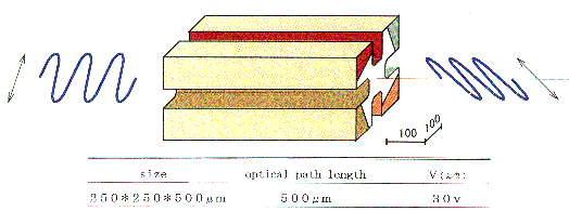
PLZT is a polycrystal
ceramics material which displays optical transparency between
infrared spectrum range near 500nm and visible spectrum range.
Combining the PLZT devise and polarizers together enable it
to operate in high speed switching. |
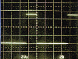
��Sample Application�� |
| Response speed |
Drive voltage |
Shutter area |
Electrostatic capacity |
| 5��sec�i��200khz�j |
71V |
10�~10mm |
0.1��F |
|
 |
|
 |
|
 |
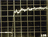
20V/div �@�@2ms/div
Drive voltage�i71V�j |
|
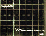
2��s/div
Rise photocurrent form |
|
2��s/div
Fall phtocurrent form |
|
�@�@ |
 |
We are selling single crystal, produced
by MTI Corp. (Material Technology International) in the
U.S.A. MTI Corp. supplies various single crystal substrates,
such as Si, �V-�X, �U-�W, oxides and alkali halides. LSAT�iLaxSr1-x�j�iAlxTa
1-x�jO3 single
crystal have been suggested for applications in high temperature
superconductors and GaN epitaxial substrates.
|
|
��LSAT
wafers specification and properties��
| �@SIZE |
�@10�~10�~0.5t�o |
�@1���~1���~0.5t�o |
�@35���~0.5t�o |
�@Other
size |
| POLISH |
�@1sp.
2sp�@�@ |
�@1sp.
2sp�@�@ |
�@1sp.
2sp�@�@ |
�@1sp.
2sp�@�@ |
| �@ORIENTATION |
�@<111>�@<100> |
�@<111>�@<100> |
�@<111>�@<100> |
�@<111>�@<100> |
| �@PRICE |
�@Estimate |
�@Estimate |
�@Estimate |
�@Estimate |
| �@DELIVERY |
�@1�`2months |
�@1�`2months |
�@1�`2months |
�@1�`2months |
| Melting point |
Density |
Growth Method |
Crystal Structure |
Lattice Constant |
| 1840���@ |
6.74 |
CZ
method |
Cubic
Structure |
a=3.868�� |
��We also supply Sapphire and SiC from
MTI Corp. Please inquire.
|

|
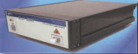 SLD-2001
series wide band light sources are infrared light sources using
Super Luminescent Diodes(SLD) to provide coverage in the C and
L band communication regions at a price much less than a regular
ASE Light Source. The basic set provides high stable diode current
and Peltier temperature control mode, however, there are optional
types, such as the APC control type, that includes a photodiode
and have an isolator added at the optical output. SLD-2001
series wide band light sources are infrared light sources using
Super Luminescent Diodes(SLD) to provide coverage in the C and
L band communication regions at a price much less than a regular
ASE Light Source. The basic set provides high stable diode current
and Peltier temperature control mode, however, there are optional
types, such as the APC control type, that includes a photodiode
and have an isolator added at the optical output.
Three core wave
lengths are available; 840nm, 1310nm, 1n3 1550nm.
You can choose various combinations for a variety of machine
types.
��Specification��
| �@Code
No. |
�@SLD-2001-(A,B,C
or D)-(option) |
| �@Optical
output morphology |
�@SMF+FC
Connector |
| �@Total
output |
�@-0.97dBm |
| �@Spectral
power density |
�@>-30dBm/nm,
1520-1600nm |
| �@Output
stability |
�@<�}0.01dB(typ.) |
| �@Outside
dimension |
�@130(H)�~440(W)�~460(D)mm |
| �@Operating
temperature |
�@10�`30�� |
| �@Storage
temperature |
�@-45�`45�� |
|

|
 |
�@�@�@PLZT
substrates polish processing
�@�@�@�@t0.03mm(10*10)�` |
|
|